- 您现在的位置:买卖IC网 > Sheet目录490 > NTMFS4836NT1G (ON Semiconductor)MOSFET N-CH 30V 11A SO8 FL
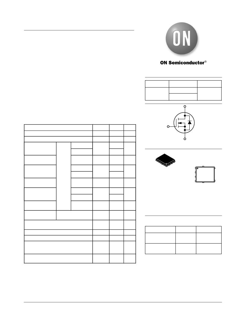
NTMFS4836N
Power MOSFET
30 V, 90 A, Single N ? Channel, SO ? 8FL
Features
? Low R DS(on) to Minimize Conduction Losses
? Low Capacitance to Minimize Driver Losses
? Optimized Gate Charge to Minimize Switching Losses
? These are Pb ? Free Devices
Applications
? Refer to Application Note AND8195/D
? CPU Power Delivery
? DC ? DC Converters
? Low Side Switching
V (BR)DSS
30 V
http://onsemi.com
R DS(ON) MAX
4.0 m W @ 10 V
6.0 m W @ 4.5 V
D (5,6)
I D MAX
90 A
MAXIMUM RATINGS (T J = 25 ° C unless otherwise stated)
Parameter
Drain ? to ? Source Voltage
Gate ? to ? Source Voltage
Symbol
V DSS
V GS
Value
30
± 20
Unit
V
V
G (4)
S (1,2,3)
S
S
G
Continuous Drain
Current R q JA
(Note 1)
Power Dissipation
R q JA (Note 1)
Continuous Drain
Current R q JA
(Note 2)
Power Dissipation
R q JA (Note 2)
Continuous Drain
Current R q JC
(Note 1)
Power Dissipation
R q JC (Note 1)
Steady
State
T A = 25 ° C
T A = 85 ° C
T A = 25 ° C
T A = 25 ° C
T A = 85 ° C
T A = 25 ° C
T C = 25 ° C
T C = 85 ° C
T C = 25 ° C
I D
P D
ID
P D
I D
P D
18
13
2.25
11
8
0.89
90
65
55.6
A
W
A
W
A
W
N ? CHANNEL MOSFET
MARKING
DIAGRAM
D
1 S
4836N
SO ? 8 FLAT LEAD AYWZZ
CASE 488AA
STYLE 1
D
A
= Assembly Location
Y
= Year
W
= Work Week
ZZ
= Lot Traceability
D
D
Pulsed Drain
Current
T A = 25 ° C,
t p = 10 m s
I DM
180
A
Operating Junction and Storage
Temperature
Source Current (Body Diode)
Drain to Source DV/DT
Single Pulse Drain ? to ? Source Avalanche
Energy (T J = 25 ° C, V DD = 50 V, V GS = 10 V,
I L = 22 A pk , L = 1.0 mH, R G = 25 W)
T J ,
T STG
I S
dV/dt
EAS
? 55 to
+150
46
6
242
° C
A
V/ns
mJ
ORDERING INFORMATION
Device Package Shipping ?
NTMFS4836NT1G SO ? 8FL 1500 /
(Pb ? Free) Tape & Reel
NTMFS4836NT3G SO ? 8FL 5000 /
(Pb ? Free) Tape & Reel
Lead Temperature for Soldering Purposes T L 260 ° C
(1/8” from case for 10 s)
Stresses exceeding Maximum Ratings may damage the device. Maximum
Ratings are stress ratings only. Functional operation above the Recommended
Operating Conditions is not implied. Extended exposure to stresses above the
Recommended Operating Conditions may affect device reliability.
1. Surface ? mounted on FR4 board using 1 sq ? in pad, 1 oz Cu.
2. Surface ? mounted on FR4 board using the minimum recommended pad size.
?For information on tape and reel specifications,
including part orientation and tape sizes, please
refer to our Tape and Reel Packaging Specifications
Brochure, BRD8011/D.
? Semiconductor Components Industries, LLC, 2012
May, 2012 ? Rev. 7
1
Publication Order Number:
NTMFS4836N/D
发布紧急采购,3分钟左右您将得到回复。
相关PDF资料
NTMFS4837NT1G
MOSFET N-CH 30V 10A SO8 FL
NTMFS4839NT3G
MOSFET N-CH 30V 9.5A SO-8FL
NTMFS4841NT3G
MOSFET N-CH 30V 8.3A SO-8FL
NTMFS4845NT3G
MOSFET N-CH 30V 13.7A SO-8FL
NTMFS4846NT3G
MOSFET N-CH 30V 12.7A SO-8FL
NTMFS4847NAT3G
MOSFET N-CH 30V 11.5A SO-8FL
NTMFS4849NT3G
MOSFET N-CH 30V 10.2A SO-8FL
NTMFS4851NT3G
MOSFET N-CH 30V 9.5A SO-8FL
相关代理商/技术参数
NTMFS4836NT3G
功能描述:MOSFET NFET 30V 90A 4MOHM RoHS:否 制造商:STMicroelectronics 晶体管极性:N-Channel 汲极/源极击穿电压:650 V 闸/源击穿电压:25 V 漏极连续电流:130 A 电阻汲极/源极 RDS(导通):0.014 Ohms 配置:Single 最大工作温度: 安装风格:Through Hole 封装 / 箱体:Max247 封装:Tube
NTMFS4837N
制造商:ONSEMI 制造商全称:ON Semiconductor 功能描述:+12 V Telecom Power Conversion Solutions
NTMFS4837NH
制造商:ONSEMI 制造商全称:ON Semiconductor 功能描述:Power MOSFET 30 V, 75 A, Single N−Channel, SO−8FL
NTMFS4837NHT1G
功能描述:MOSFET NFET S08FL 30V 74A 5mOhm RoHS:否 制造商:STMicroelectronics 晶体管极性:N-Channel 汲极/源极击穿电压:650 V 闸/源击穿电压:25 V 漏极连续电流:130 A 电阻汲极/源极 RDS(导通):0.014 Ohms 配置:Single 最大工作温度: 安装风格:Through Hole 封装 / 箱体:Max247 封装:Tube
NTMFS4837NHT3G
功能描述:MOSFET NFET S08FL 30V 74A 5MO RoHS:否 制造商:STMicroelectronics 晶体管极性:N-Channel 汲极/源极击穿电压:650 V 闸/源击穿电压:25 V 漏极连续电流:130 A 电阻汲极/源极 RDS(导通):0.014 Ohms 配置:Single 最大工作温度: 安装风格:Through Hole 封装 / 箱体:Max247 封装:Tube
NTMFS4837NT1G
功能描述:MOSFET NFET 30V 16A 5MOHM RoHS:否 制造商:STMicroelectronics 晶体管极性:N-Channel 汲极/源极击穿电压:650 V 闸/源击穿电压:25 V 漏极连续电流:130 A 电阻汲极/源极 RDS(导通):0.014 Ohms 配置:Single 最大工作温度: 安装风格:Through Hole 封装 / 箱体:Max247 封装:Tube
NTMFS4837NT3G
功能描述:MOSFET NFET 30V 16A 5MOHM RoHS:否 制造商:STMicroelectronics 晶体管极性:N-Channel 汲极/源极击穿电压:650 V 闸/源击穿电压:25 V 漏极连续电流:130 A 电阻汲极/源极 RDS(导通):0.014 Ohms 配置:Single 最大工作温度: 安装风格:Through Hole 封装 / 箱体:Max247 封装:Tube
NTMFS4839N
制造商:ONSEMI 制造商全称:ON Semiconductor 功能描述:Power MOSFET 30 V, 66 A, Single N−Channel, SO−8FL
